Research publication · TerahertzTerahertz radiation is electromagnetic energy commonly associated with frequencies around 0.1 to 10 THz, between microwaves and infrared, where many materials reveal distinctive propagation, absorption, and imaging behavior. More absorbers and detectors
Theoretical and experimental studies of metallic grids absorption: Application to the design of a bolometer
A thermal detector is only as effective as the surface that turns incident radiation into heat. For a conventional metallic film, high absorption may require a thickness of only a few nanometres. Such films are difficult to reproduce, and their electrical and mechanical properties can vary sharply with deposition conditions. This paper explores a more controllable alternative: pattern a thicker metal layer as a grid, then use the geometry of that grid to obtain the effective electrical resistance required for absorption. The study connects electromagnetic theory, finite-element simulation and measurements from radio frequencies to 0.3 THz, providing a design framework rather than claiming a finished bolometer.
Featured visual: Contextual research figure from âRoom temperature thermopile THz sensorâ. It illustrates a closely related terahertzTerahertz radiation is electromagnetic energy commonly associated with frequencies around 0.1 to 10 THz, between microwaves and infrared, where many materials reveal distinctive propagation, absorption, and imaging behavior. More topic and is not a figure from the publication discussed on this page. Source publication.
Visuals are drawn from the Airtable research archive. Figure numbering, rights and interpretation should be checked against the original publication before republication outside this site.
Engineering resistance through geometry
The key idea is to separate the metal’s intrinsic resistivity from the electromagnetic response of the patterned sheet. Current is forced to flow through narrow lines instead of a continuous film, so the grid behaves as a layer with an equivalent resistivity determined by line width, period, thickness and conductivity. Adjusting these dimensions can therefore reproduce the impedance of an extremely thin homogeneous absorber while retaining a metal thickness compatible with established lithography and lift-off processes.
The authors formulate the absorber as part of a multilayer stack. At every dielectric or metallic interface, the tangential electric and magnetic fields must remain continuous. Solving those boundary conditions recursively gives the fields inside the stack and, from them, the reflected, transmitted and absorbed fractions of the incident power. The treatment also refines the description of current within the conductor. Instead of assuming a symmetric current distribution limited by an ordinary skin depth, it uses an exponential profile characterized by an equivalent skin depth that depends on conductivity and grid geometry.
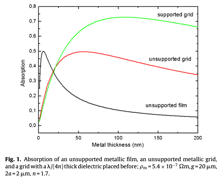
For a grid much thinner than this equivalent skin depth, and with a period small enough for diffraction to be neglected, the resulting expression relates absorption directly to grid impedance and free-space impedance. The simplification is valuable because it makes the influence of geometry explicit. Yet the authors do not stop at that ideal regime. A practical absorber is often carried by a dielectric, and its period may not be vanishingly small relative to wavelength. To handle those cases, the grid is represented by a lumped electrical impedance containing reactive and resistive terms, while the support is represented as a transmission-line section. This equivalent-circuit view incorporates substrate interference and diffraction more realistically.
Validation at terahertz and radio frequencies
Two-dimensional simulations in the RF module of COMSOL Multiphysics were first compared with the analytical model under plane-wave illumination. In the low-diffraction regime, the calculated absorption, transmission and reflection agreed closely. This numerical cross-check matters because it tests whether a geometrically patterned conductor can legitimately be replaced by a homogeneous equivalent layer for the selected range of dimensions.
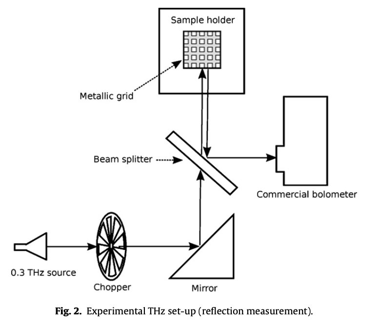
The terahertzTerahertz radiation is electromagnetic energy commonly associated with frequencies around 0.1 to 10 THz, between microwaves and infrared, where many materials reveal distinctive propagation, absorption, and imaging behavior. More experiment used titanium grids fabricated on glass by clean-room lithography. The deposited titanium was 160 nm thick, while line widths and grid spacing were varied across the samples. At 0.3 THz, a source-and-bolometer arrangement measured transmitted and reflected power; absorption followed from the incident-power balance. The measured trends closely followed the multilayer calculations. The remaining differences were associated with uncertainties such as substrate thickness and the actual electrical properties of the deposited titanium, rather than hidden fitting parameters being presented as universal constants.
A second experiment addressed structures whose overall dimensions were smaller relative to wavelength. Grids measuring 1 cm and 2 cm were placed in a custom 50-ohm TEM guide and characterized between 900 MHz and 10 GHz. Scattering measurements allowed the equivalent resistivity to be inferred. It varied with the ratio between grid size and wavelength, demonstrating that simple bulk-resistivity scaling is not sufficient once the patterned area becomes electromagnetically small. The RF test is not a substitute for a terahertzTerahertz radiation is electromagnetic energy commonly associated with frequencies around 0.1 to 10 THz, between microwaves and infrared, where many materials reveal distinctive propagation, absorption, and imaging behavior. More detector measurement, but it isolates a scaling effect that is difficult to study with the same precision in the higher-frequency apparatus.
Relevance to room-temperature terahertz detection
The immediate application is the absorber of a bolometer or thermopile. By choosing geometry rather than relying only on film thickness, a designer can tune dissipation while also considering thermal mass, mechanical support and fabrication yield. The work provides experimentally supported rules for that first stage of detector design. It does not report a complete detector’s responsivity, noise-equivalent power or response time, and it does not establish performance for every metal and substrate. The terahertzTerahertz radiation is electromagnetic energy commonly associated with frequencies around 0.1 to 10 THz, between microwaves and infrared, where many materials reveal distinctive propagation, absorption, and imaging behavior. More validation used titanium on glass, while the subwavelength analysis depended on accurate knowledge of the TEM fixture and substrate.
Within those boundaries, the study is significant because it links electromagnetic absorption to manufacturable dimensions. That bridge later supports room-temperature THz sensor prototypes using metallic grids on thermally isolated membranes. It also illustrates a productive collaboration between microfabrication and thermal-sensor specialists at FEMTO-ST and terahertzTerahertz radiation is electromagnetic energy commonly associated with frequencies around 0.1 to 10 THz, between microwaves and infrared, where many materials reveal distinctive propagation, absorption, and imaging behavior. More instrumentation researchers in Montpellier. The result is best understood as a validated modeling and measurement toolkit: it reduces guesswork when selecting absorber geometry, while leaving detector integration and optimization as separate engineering tasks.
Bibliographic reference
Recommended citation: Ben Mbarek, S., Baron, T., Euphrasie, S., Cretin, B., Vairac, P., Adam, R., Chusseau, L., Guillet, J.-P., & Penarier, A. (2009). Theoretical and experimental studies of metallic grids absorption: Application to the design of a bolometer. Procedia Chemistry, 1(1), 1135-1138. https://doi.org/10.1016/j.proche.2009.07.283
Publisher: Elsevier. Airtable record: recY0MwdNx2Ne09Db.